AI CERTS
2 months ago
AI Memory Development Accelerates at Applied Materials EPIC
Micron, SK hynix, and Samsung will be the first tenants inside the new facility. Each company seeks faster paths toward next-gen memory products demanded by AI workloads. Applied offers the process expertise, metrology tooling, and capital equipment to shrink experimental cycles. Therefore, the announcement does not signal that Applied will manufacture chips itself. Instead, the company maintains its traditional supplier role while deepening co-innovation programs.
Such nuance is crucial because early coverage mischaracterized the news as Applied entering memory production. Consequently, understanding the actual strategy behind AI Memory Development matters for investors and engineers alike. Moreover, the scale and structure of the new hub illustrate evolving collaboration patterns across the semiconductor supply chain.
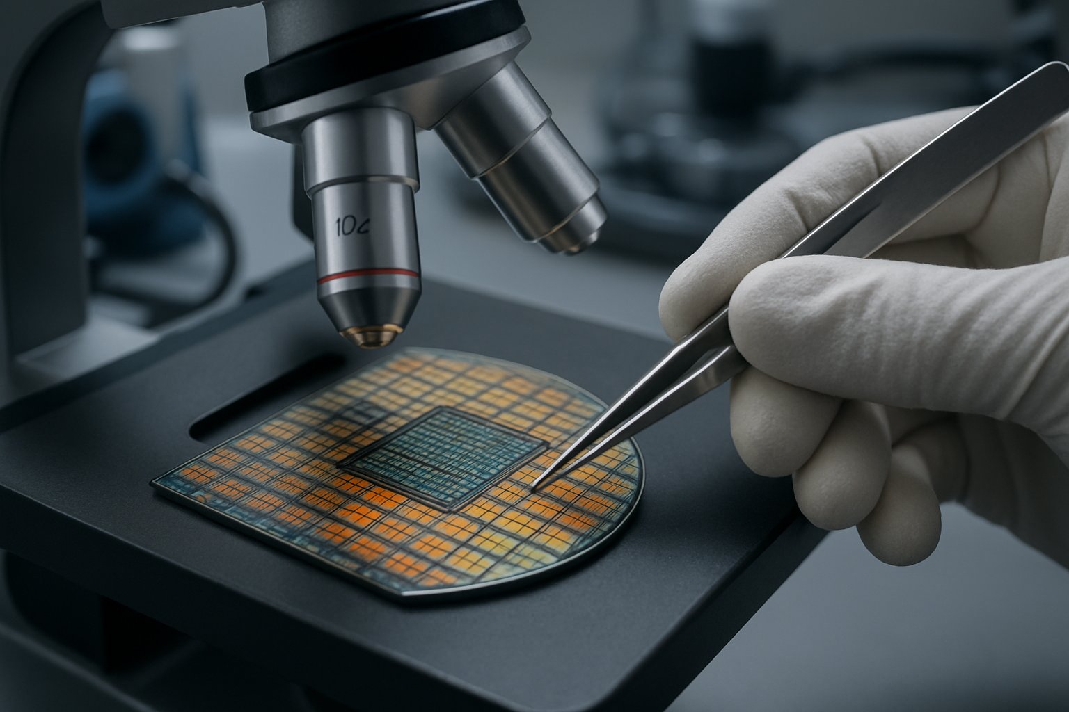
EPIC Center Overview Today
Applied describes the EPIC center as a living lab for materials engineering. Moreover, the company plans a capital investment of about $5 billion to build specialized cleanrooms and pilot lines. This proximity reduces feedback loops and lowers R&D cycle time for next-gen memory prototypes. Consequently, Applied asserts that ideas can move from simulation to silicon in months rather than years.
In short, the facility embeds tooling and talent inside one adaptable site. That structure compresses development cycles and cuts costly iterations. Next, we examine the market forces driving this urgency.
Industry Drivers And Demand
Omdia pegged industry revenue at $216.3 billion in Q3 2025, with memory leading growth. Moreover, high bandwidth memory shortages have constrained accelerator shipments to hyperscale data centers. AI training jobs crave enormous capacity and speed, making DRAM and HBM strategic commodities. Consequently, chipmakers scramble to deliver next-gen memory nodes with wider buses and lower energy per bit.
- HBM market grew 57% year-over-year in 2025, TrendForce reports.
- AI servers consume up to 700GB of DRAM per node, according to Omdia.
- Memory spending accounted for 38% of 2025 wafer fab equipment orders.
These metrics underline an urgent commercial incentive. Sustained demand promises return on every EPIC center investment supporting AI Memory Development. Understanding how partnerships channel that capital is the next essential step.
Partnership Structure Explained Clearly
Applied signed multi-year agreements with Micron, SK hynix, and Samsung. Additionally, each memory maker will colocate engineers in Silicon Valley for joint process R&D. The program follows a lab-to-fab model linking Micron’s Boise facility to the California hub. Meanwhile, SK hynix focuses on 3D integration and advanced packaging alongside Applied technologists. These joint teams form the human backbone of AI Memory Development.
Samsung, announced earlier, remains a founding collaborator and provides baseline HBM process flows. Nevertheless, Applied retains its role as equipment supplier rather than a competing memory vendor. IP governance policies partition data, ensuring sensitive layouts stay within company-specific work areas.
Together, those agreements create a shared toolbox without merging corporate roadmaps. This model mirrors successful foundry alliances seen in logic nodes. Technical priorities now deserve a closer look.
Technology Focus And Roadmap
The initial roadmap targets DRAM scaling, HBM stacking, and higher density NAND. Moreover, Applied will refine hybrid bonding to stack eight or more DRAM dies. Process control improvements aim to double vertical alignment accuracy. Consequently, next-gen memory bandwidth could exceed 2TB per second per package. Such innovations underpin scalable AI Memory Development across data centers. Interactive R&D dashboards will track defect density daily.
Energy efficiency remains another pillar. Engineers will co-optimize materials, via dimensions, and cooling paths to cut picojoules per bit. Additionally, NAND collaboration pursues higher layer counts while controlling stress in ultra-tall stacks.
These technical milestones provide concrete yardsticks for overall memory innovation progress. Successful demonstrations will shift focus from the lab to high volume production. Compliance issues, however, could slow that shift.
Regulatory And Geopolitical Risks
In February 2026, the U.S. BIS fined Applied $252 million for prior export violations. Therefore, the company now subjects every shipment to additional screening. Micron and SK hynix must ensure joint experiments stay within license boundaries. In contrast, Samsung faces separate U.S. approval processes for certain equipment transfers.
Moreover, Washington continues tightening controls on advanced memory tools bound for Chinese fabs. Consequently, Applied must navigate evolving policy while courting global customers. Any misstep could jeopardize EPIC center timelines and associated investment. Compliance lapses could derail AI Memory Development timelines.
Regulatory headwinds add cost and uncertainty. Nevertheless, strong demand forces stakeholders to push ahead. Evaluating business benefits therefore becomes imperative. The following section assesses tangible upside.
Benefits For AI Ecosystem
The collaboration hub promises faster qualification of equipment recipes. Furthermore, shared pilot lines can reduce capital duplication across three rival memory firms. Analysts predict two main gains for AI Memory Development adopters.
- Lower time to market, potentially three quarters faster than historical averages.
- Up to 15% energy per bit savings through joint materials tuning.
Additionally, Applied gains recurring revenue as each partner upgrades tool sets. Micron and SK hynix secure early access to process breakthroughs, boosting competitive positioning. These benefits strengthen the business case. Yet strategic alignment must translate into clear roadmaps. Key takeaways and future outlook conclude the analysis.
Strategic Takeaways And Outlook
AI Memory Development now sits at the intersection of materials science, economics, and geopolitics. EPIC center funding of $5 billion represents a landmark investment in U.S. semiconductor infrastructure. Moreover, co-innovation agreements distribute risk and enable faster iteration on next-gen memory stacks. Nevertheless, trade compliance will continue shaping project scope and timetables. Shared R&D data may also inform government funding requests.
Ultimately, success will depend on hitting measurable milestones in bandwidth, energy, and cost. Industry professionals should monitor quarterly updates from Applied and its partners. Professionals can enhance their expertise with the AI+ Quantum™ certification. Such credentials align with technical demands emerging from AI Memory Development projects.
Conclusion And Next Steps
Applied's expanded collaborations reframed the narrative around AI Memory Development. The company remains an equipment powerhouse, yet its influence on chip architectures keeps growing. Moreover, Micron, SK hynix, and Samsung gain earlier access to essential process knowledge. Consequently, data center operators may see faster performance gains and lower power footprints.
Nevertheless, regulatory scrutiny and supply tightness remain watchpoints for every stakeholder. Therefore, professionals should track milestone disclosures and consider upskilling before adoption ramps. Explore the linked certification to deepen expertise and stay ahead of industry shifts.
Disclaimer: Some content may be AI-generated or assisted and is provided ‘as is’ for informational purposes only, without warranties of accuracy or completeness, and does not imply endorsement or affiliation.


