

AI CERTS
7 months ago
OFE2: A Hardware Processing Engine Surpassing 12.5 GHz Optics
Moreover, its per-multiplication latency clocks in at just 250.5 picoseconds. That figure undercuts many electronic field-programmable gate array (FPGA) baselines by double-digit nanoseconds. In this report, we unpack the science, architecture, and commercial stakes behind the system. Throughout, we assess how this photonic Hardware Processing Engine could reshape ultra-low latency workloads. Additionally, we weigh integration hurdles that still separate lab optics from production deployments. Professionals seeking deeper mastery can validate skills through the linked AI Engineer certification.
New Diffraction Computing Breakthrough
Integrated photonics has marched forward, yet surpassing 10 GHz remained elusive until recently. However, the OFE2 prototype shattered that barrier during October 2025 peer-reviewed tests. The Tsinghua team reported 12.5 GHz sustained operation, verified with on-chip electro-optic probes. Moreover, independent analysts hailed the demonstration as a credible inflection point for diffractive computing.
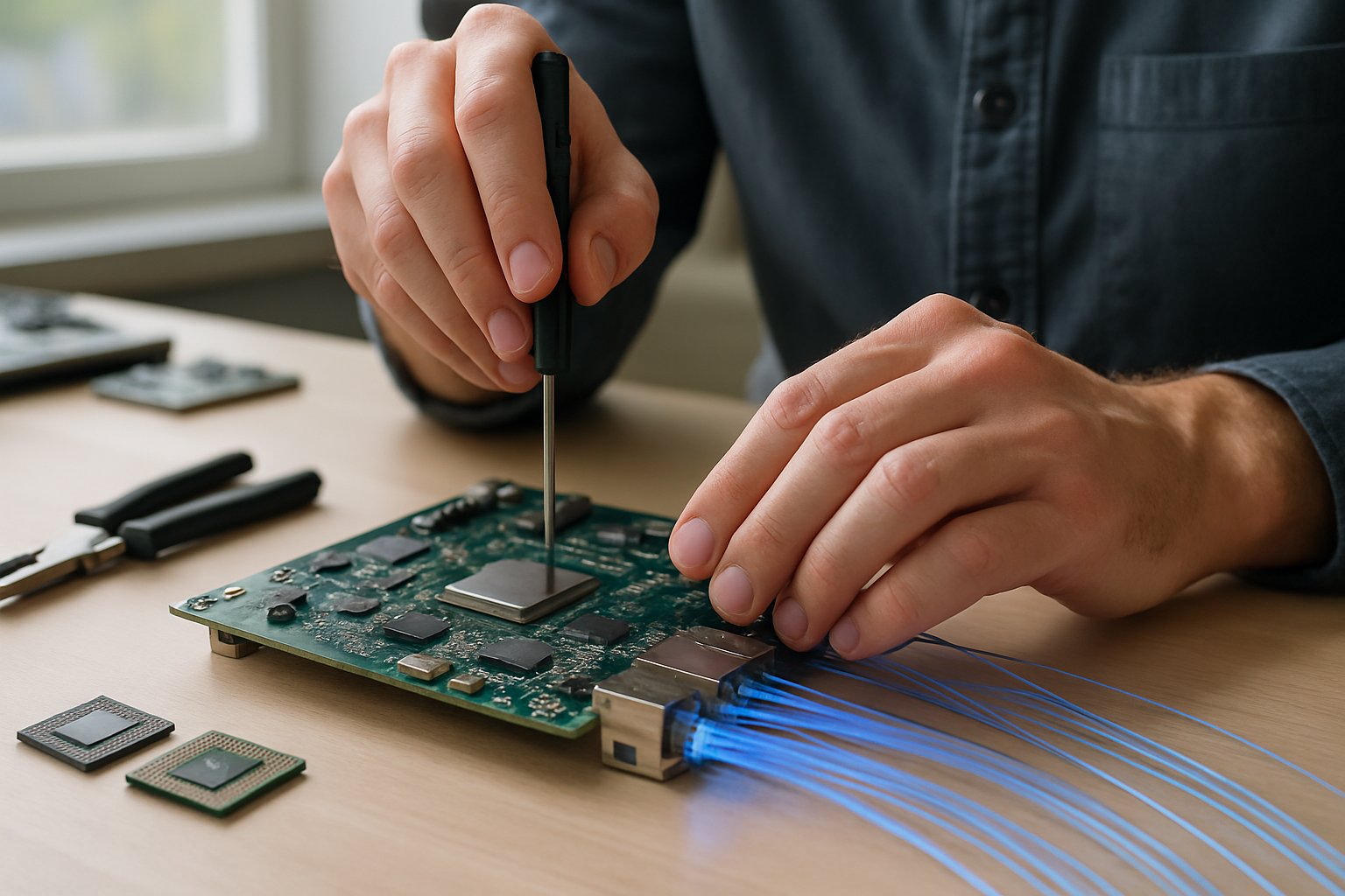
At the heart lies a patterned diffraction plate that manipulates coherent Light to perform linear algebra. Consequently, optical power steers toward output waveguides in proportions representing matrix coefficients. This physical parallelism gives the Hardware Processing Engine a natural edge over serial electronic multipliers. Nevertheless, optical inputs must arrive phase-aligned, or accuracy degrades rapidly. The group solved that challenge with an innovative serial-to-parallel deserializer built from tunable splitters and delay lines.
The prototype therefore establishes a fresh benchmark for speed in coherent photonic circuits. Consequently, attention now turns to hard performance numbers.
Key Performance Metrics Revealed
Quantitative evaluation separates marketing hype from engineering substance. Therefore, we summarize the peer-reviewed figures that define OFE2's laboratory achievement. The Hardware Processing Engine recorded 250 GOPS throughput at 0.1214-watt core power. Moreover, energy cost reached only 9.71 picojoules per operation, yielding 2.06 TOPS per watt.
- 12.5 GHz operating frequency validated on prototype board.
- ≈250.5 picoseconds latency per matrix-vector multiplication.
- End-to-end chain latency measured at 82.21 nanoseconds.
- Energy efficiency of 2.06 TOPS/W in core tests.
- 250 GOPS sustained throughput under benchmark conditions.
In contrast, the authors modeled a 94-nanosecond FPGA baseline under similar workload parameters. Consequently, OFE2 enjoyed an 11.8-nanosecond lead for full pipeline latency. These deltas matter greatly in high-frequency trading and medical imaging. However, results depend on matrix dimension, sparsity, and data conversion overheads. Precise knowledge of the architecture clarifies those dependencies. Subsequently, we explore the silicon layout.
Architecture Behind Photonics Engine
Every nanosecond gain stems from meticulous photonic layout decisions. Firstly, the deserializer converts a serial input stream into eight phase-aligned optical branches. Consequently, each branch drives a dedicated region of the diffraction operator without temporal skew. The operator itself is a 510-micrometer plate etched to redirect coherent Light into predefined exit ports. Meanwhile, integrated heaters and monitoring taps maintain phase stability against thermal drift.
The Hardware Processing Engine integrates modulators at entry points, permitting rapid amplitude and phase encoding. Moreover, the team fabricated delay lines using silicon nitride, minimizing propagation loss. Output waveguides couple to transimpedance amplifiers, closing the optical-electronic loop for digitization. In contrast, earlier photonic efforts relied on bulky external serializers that limited practical frequency.
This tight integration underpins the reported 12.5 GHz ceiling. Therefore, understanding application fit becomes the next priority.
Broad Industry Applications Potential
Latency sensitive domains stand to benefit first. For instance, the paper presented an optical edge extractor that pre-filters medical CT scans. Consequently, downstream convolutional networks needed fewer layers, shrinking electronic compute budgets. Similarly, quantitative traders prize nanosecond advantage; the Hardware Processing Engine delivered profitable signals in simulations. Moreover, defense radar and autonomous driving could exploit immediate feature maps for situational awareness.
Tsinghua researchers argue that energy efficiency also favours remote sensing satellites, where power budgets are scarce. Nevertheless, large-scale adoption hinges on manufacturability and software tooling. Professionals wanting a competitive edge can validate photonic skills. They can pursue the AI Engineer™ certification for credible proof.
Use cases are compelling yet conditional. Therefore, challenges deserve balanced scrutiny.
Challenges And Next Steps
High figures can mislead if system costs erase optical gains. Firstly, electro-optic conversions still introduce latency and energy penalties beyond core measurements. Moreover, phase stability demands packaging that resists vibration and temperature drift. In contrast, electronic GPUs tolerate far wider environmental swings. Analysts also caution that benchmarking across disparate matrix sizes hampers fair comparisons.
Tsinghua plans to explore wavelength division multiplexing to scale throughput without area penalties. Subsequently, third-party labs must replicate OFE2 data under standardized workloads. Meanwhile, manufacturing partners will need reliable yield for the diffraction operator. Nevertheless, the Hardware Processing Engine concept remains attractive for collaboration.
Open challenges invite joint academic-industry efforts. Consequently, strategic lessons emerge for practitioners.
Strategic Takeaways For Professionals
Adopting any Hardware Processing Engine demands holistic assessment, not isolated core figures. Therefore, compute architects should evaluate data-flow, software support, and environment constraints. In contrast, ignoring integration costs risks disappointing performance in production. Key due-diligence questions include replication status, packaging roadmap, and interface standards. Moreover, investors must compare returns against maturing electronic ASICs and emerging quantum accelerators.
Critical Evaluation Checklist Points
- Request independent latency measurements.
- Verify efficiency under full workloads.
- Inspect thermal stability data.
- Confirm manufacturing partner commitments.
Professionals who master these optics may steer future system roadmaps. Furthermore, early adoption can differentiate products in saturated markets.
In summary, OFE2 signals that coherent Light computing is maturing rapidly. The Hardware Processing Engine posts impressive latency and efficiency wins in controlled environments. However, production impact will depend on packaging, toolchains, and measured system gains. Nevertheless, forward-thinking teams should evaluate the Hardware Processing Engine against their most latency-sensitive pipelines. Consequently, early pilots could capture competitive advantage before standards converge. Professionals can showcase readiness to deploy a Hardware Processing Engine by securing respected certifications. Explore the linked AI Engineer course to begin that journey today.
Disclaimer: Some content may be AI-generated or assisted and is provided ‘as is’ for informational purposes only, without warranties of accuracy or completeness, and does not imply endorsement or affiliation.


