AI CERTS
2 hours ago
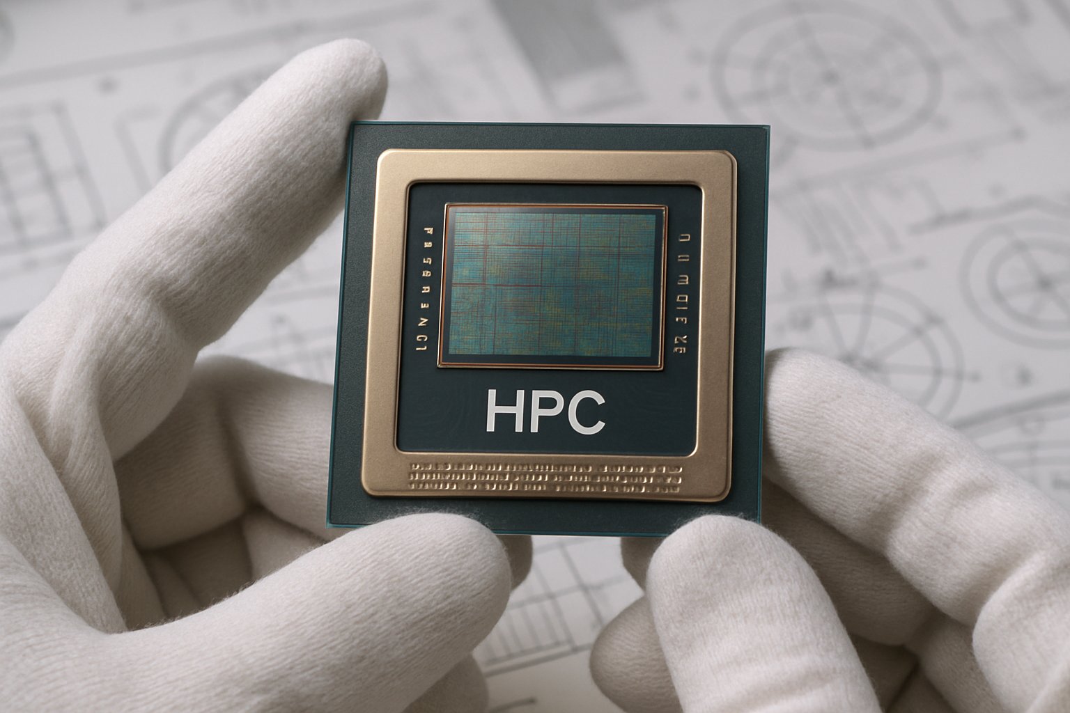
Micron Partnership Fuels HPC Chip Research at EPIC Center
The facility, dubbed EPIC, represents a $5 billion lab-to-fab campus scheduled to open this year. Industry watchers consider the deal a flagship example of HPC Chip Research driving cross-company investment. Meanwhile, Micron will leverage its Boise innovation hub to validate materials and process recipes in parallel. Therefore, engineers expect faster qualification cycles and earlier customer sampling.
In contrast, traditional siloed models often stretch memory development timelines by several quarters. Additionally, hyperscaler capital spending on AI infrastructure—Bloomberg pegs 2026 budgets near $650 billion—creates urgent pull for high-bandwidth memory chips. Nevertheless, supply constraints remain. The Micron partnership intends to relieve those bottlenecks and secure domestic technology leadership.
Market Drivers Surge Forward
Global demand for AI training servers keeps snowballing. Consequently, hyperscalers forecast record equipment budgets that surpass most national GDPs. Bloomberg estimates 2026 aggregate capex at roughly $650 billion. Moreover, a sizable share targets GPUs and the stacked memory that feeds them. TrendForce data show HBM shipments expanding double digits each quarter. Therefore, Applied and Micron see a lucrative opening. The Micron partnership positions both firms to capture share before rivals ramp.
Meanwhile, elevated DRAM pricing boosts Micron’s cash flow, funding additional pilot lines. In contrast, equipment makers benefit when novel process steps migrate from research to volume tools. HPC Chip Research becomes an execution race, not a science experiment. Additionally, regulators favour domestic capacity given ongoing export controls. These market currents make a U.S. lab-to-fab hub strategically timely.
The numbers illustrate intense memory appetite and rising stakes. However, drivers alone do not guarantee execution success.
Consequently, understanding the exact collaboration scope is essential.
Partnership Scope Explained Clearly
Applied Materials labeled Micron a founding partner for the EPIC Center. Moreover, the companies will co-locate engineers that specialize in deposition, etch, and advanced packaging. They intend to share simulation data, prototype wafers, and in-line metrology dashboards. Consequently, decisions that previously required weeks can occur within hours. HPC Chip Research thrives on that compressed feedback loop. Additionally, Micron partnership commitments include joint investment in beta equipment and materials.
The arrangement spans DRAM, HBM4, and NAND, plus related chip-development workflows such as lithography targeting 3D structures. Meanwhile, Boise staff will mirror selected process experiments to validate factory compatibility. EPIC program governance reportedly includes confidentiality firewalls to protect each participant’s intellectual property. Nevertheless, Applied will reuse positive findings across its broader customer base after appropriate windows lapse.
The defined scope extends well beyond a marketing alliance. Therefore, technical deliverables carry measurable milestones.
Subsequently, we examine how the research touches compute performance.
HPC Chip Research Impact
Low-power, high-bandwidth memory sits near the top of AI system bottlenecks. Moreover, every additional terabyte per second slashes inference latency. Micron’s HBM revenue nearly hit $2 billion in fiscal Q4 2025, underscoring commercial urgency. Applied’s process engineers claim that novel materials can cut per-bit energy by 15 percent. Consequently, HPC Chip Research inside EPIC aims to integrate those films into production-grade DRAM stacks. The program also explores wafer-level bonding to fuse memory chips directly onto compute dies.
Additionally, chip-development efforts target thermal management innovations to dissipate rising power densities. Memory chips that survive hotter junctions extend package life and lower cooling costs. In contrast, legacy designs suffer throttling under sustained AI workloads. Therefore, the partnership’s technical agenda aligns perfectly with hyperscaler pain points.
Performance gains translate into competitive advantage and lower TCO. Nevertheless, timeline clarity remains crucial.
We now review the planned lab-to-fab schedule.
Technology Focus Areas Detailed
Project leaders have prioritized four intertwined workstreams.
- Materials innovations for DRAM capacitors and HBM dielectric stacks
- 3D advanced packaging schemes that shrink signal paths
- NAND cell architecture tweaks supporting AI-aware storage tiers
- Inline analytics powered by machine learning for faster chip-development feedback
Furthermore, each stream operates under joint sprint cycles lasting eight weeks. Engineers alternate between the EPIC cleanroom and Micron’s pilot lines. Consequently, discoveries migrate quickly into design-of-experiments on 300 mm wafers. HPC Chip Research appears tenacious here, appearing at every whiteboard review. Meanwhile, Applied’s tool designers capture upgrade requirements that could lift future equipment orders. Additionally, professionals can enhance their expertise with the AI+ Quantum Specialist™ certification, ensuring skill relevance as architectures evolve.
Lab-to-Fab Timeline Roadmap Details
Applied executives insist the first EPIC modules will power on during Q3 2026. Moreover, early DRAM test vehicles should exit the line within six months. Micron partnership leaders have earmarked Boise capacity for correlated reliability testing. Consequently, volume-ready process flows could reach customer production ramps by mid-2027. Nevertheless, HPC Chip Research dashboards will update stakeholders monthly. Therefore, continuous risk assessment accompanies every milestone.
The roadmap sets aggressive but plausible targets. However, execution discipline will determine actual delivery.
Intellectual property governance poses the first challenge. Moreover, multiple device makers will share EPIC floor space, increasing leakage risks. Applied claims strict data segmentation policies, yet independent audits are planned. Additionally, commercialization timing depends on tool maturity and parts logistics. Supply shortages for advanced EUV photoresists could hinder chip-development progress. In contrast, regulatory hurdles may arise if export controls tighten for certain deposition technologies.
Consequently, both firms maintain government affairs teams to monitor policy shifts. Program budgets also scale with customer demand; market softness would delay capital expansion. Nevertheless, HPC Chip Research efforts often weather such storms through adaptive planning.
These uncertainties highlight why transparent metrics matter. Subsequently, market observers track analyst sentiment closely.
Strategic Implications Ahead Unveiled
Wall Street reacted quickly to the announcement. TD Cowen and Craig-Hallum each reiterated outperform ratings on Applied, citing probable equipment pull-through. Moreover, investors view the Micron partnership as a hedge against cyclical swings in commodity memory chips. EPIC, by functioning as a neutral co-innovation hub, could also influence policy debates over domestic semiconductor incentives.
Consequently, U.S. lawmakers may reference the project while shaping future CHIPS Act allocations. HPC Chip Research thus intersects finance and geopolitics. Additionally, SK hynix and Samsung have signaled intent to join EPIC, raising questions about competitive dynamics. In contrast, smaller fabless firms wonder about access tiers and cost structures. Therefore, Applied might launch affiliate programs to broaden participation.
Strategic ripple effects extend beyond the founding duo. However, the next earnings cycles will reveal concrete financial impacts.
The story now converges toward key takeaways.
Conclusion And Next Steps
Applied Materials and Micron have transformed a press release into a bold execution plan. Moreover, the $5 billion Silicon Valley center underpins an accelerated model for HPC Chip Research, memory chips design, and chip-development validation. Consequently, hyperscalers may enjoy faster, cheaper, and cooler AI servers. Nevertheless, IP safeguards, supply logistics, and regulatory currents remain pivotal variables.
Professionals aiming to contribute should monitor tool readiness, extended roadmap milestones, and upcoming JEDEC standards meetings. Furthermore, investing in continuous education, such as the linked quantum certification, reinforces market value. In contrast, ignoring the rapid shift risks obsolescence. Therefore, stay informed, engage with ecosystem forums, and prepare to capitalize on the coming memory renaissance.
Take the next step today: deepen your skills, follow EPIC updates, and position yourself at the forefront of AI memory innovation.


