AI CERTS
2 months ago
CMOS Photonic Chip Advances Quantum Computing Scaling
This article unpacks the technology, market implications, and strategic steps leaders should monitor during the next development phase. Consequently, engineers focused on optical interconnects could soon influence quantum roadmaps without drastic process changes. Nevertheless, fundamental challenges such as uniformity, detector integration, and packaging still demand coordinated effort. Understanding the new CMOS Photonic Chip will help professionals assess opportunities, risks, and required skills. Furthermore, the research offers a concrete case study for government programs prioritizing domestic quantum supply chains. Read on for a clear technical breakdown, market context, and actionable recommendations.
CMOS Foundry Breakthrough Explained
The Nature Electronics paper documents the first electronic-photonic system fabricated in a commercial 45-nm CMOS line. Researchers from Boston University, UC Berkeley, and Northwestern co-designed photonic, electronic, and thermal blocks within standard design rules. Consequently, the chip integrates waveguides, microring resonators, photodiodes, heaters, and mixed-signal electronics on one die.
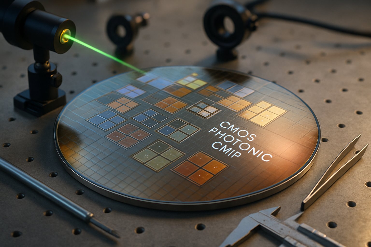
Each Photonic Chip hosts twelve independent microring photon-pair sources, arranged as miniature “quantum light factories.” Meanwhile, Vernier filters deliver 95 dB pump rejection with under 1 dB insertion loss. Such suppression ensures clean quantum channels despite the bright classical pump laser.
Thermal drift traditionally ruins microring alignment within minutes. However, embedded photodiodes measure resonance shifts, while local heaters retune rings in real time. Therefore, the device holds its quantum spectral shape for hours without external instruments.
Importantly, the complete system occupies roughly one square millimeter, matching the footprint of mainstream microcontrollers. That density signals a path toward wafer-level Scaling across thousands of sources.
The CMOS integration proves quantum photonics can ride industrial fabrication flows. Next, we examine how feedback electronics enact this stability.
On-Chip Feedback Control Strategy
Active stabilization constitutes the technical heart of the breakthrough. Embedded analog front-ends convert photodiode currents into digital error signals every microsecond. Subsequently, on-chip microcontrollers compute heater updates, closing the loop at kilohertz rates.
In contrast, earlier laboratory rigs used off-chip oscilloscopes and bulky temperature stages for similar tasks. Those peripherals limited experiment duration and raised capital costs. Moreover, cable parasitics capped loop bandwidth.
Integrated Laser Control Advances
Integrated Laser Control keeps pump wavelength and ring resonance synchronized within picometers. The algorithm measures cavity transmission spectral slopes, then predicts required heater currents. Consequently, photon-pair sources remain phase-matched even when ambient temperature drifts several degrees.
The team achieved concurrent stabilization of all twelve sources, demonstrating deterministic multiplexing possibilities. Future silicon photonics chiplets could replicate the approach to manage hundreds of rings.
Real-time Laser Control removes a notorious Bottleneck in photonic architectures. With stabilization addressed, market analysts are evaluating commercial viability.
Market Impact And Scaling
Mass-manufacturable photon sources reshape cost curves for Quantum Computing hardware vendors. GlobalFoundries already ships optical interconnect wafers at multi-thousand-wafer volumes. Therefore, adding quantum structures leverages existing tooling without major capital expenditure.
Market researchers expect silicon photonics revenues to exceed five billion dollars by 2030. Additionally, specialized photonic quantum segments could grow from one to seven billion dollars between 2030 and 2036. Although forecasts vary, all scenarios demand reliable Scaling of component yields.
Competition is heating up. Start-ups such as PsiQuantum pursue larger photonic processors, while legacy chipmakers test integrated detectors. Consequently, supply-chain partners seek standards for packaging, fiber coupling, and thermal management.
- Chip area: 1 mm × 1 mm die
- Photon-pair sources: 12 per Photonic Chip
- Pump suppression: 95 dB on-chip
- Filter loss: under 1 dB
The economic narrative hinges on high-volume Scaling and reduced per-bit costs. However, several engineering hurdles remain, as the next section details.
Addressing Technical Bottleneck Challenges
Device variability still threatens uniform performance. The study measured over two-fold differences in pair generation between best and worst rings. Such dispersion reduces interference visibility across multiplexed sources, an issue critical for fault-tolerant Quantum Computing.
Limited heater tuning range inside the 45 nm flow also constrained alignment yield. Moreover, dense heater placement produced thermal crosstalk among adjacent resonators. Engineers plan wider phase-shifter windows and improved metallization stacks for future revisions.
Detector technology presents another Bottleneck. Single-photon detectors often require cryogenic environments incompatible with standard CMOS packaging. Hybrid integration or micromachined cavities may bridge that thermal gap.
Packaging remains challenging, especially for aligning fiber arrays with micron-scale waveguides. Nevertheless, the photonics industry already sells co-packaged optics, offering transferable tooling. Consequently, partners expect rapid learning cycles once pilot modules ship.
By confronting variability, detection, and packaging, the team tackles the remaining Bottleneck head-on. The roadmap section explains how future revisions could transform prototypes into shipping parts.
Roadmap Toward Mass Production
The authors outline a three-phase plan for productization. Initially, they will package single chips inside fiber-pigtailed modules for network demonstrations. Subsequently, multi-chip interference tests will validate source indistinguishability at wafer scale.
Phase two targets integrating Superconducting Nanowire Single-Photon Detectors using flip-chip bonding. Additionally, cryogenic packaging concepts borrowed from AI accelerators may ease thermal constraints. Integrated Laser Control loops will migrate to dedicated digital signal processors for greater flexibility.
Final phase envisions heterogeneous chiplets attached to larger compute substrates through optical interposer fabrics. Here, mature silicon photonics assembly lines would supply the needed alignment accuracy. Therefore, supply-chain risk decreases as conventional contract manufacturers join the process.
Throughout all phases, rigorous process control must guarantee micro-scale uniformity across entire wafers. Market adoption will stall without predictable Scaling statistics. Consequently, statistical process control dashboards are under development.
The staged roadmap illustrates pragmatic engineering, bridging laboratory proof to manufacturable volume. Leaders should now consider how these timelines influence investment priorities.
Strategic Takeaways For Leaders
C-suite executives should watch three pivotal metrics. First, track wafer yield for repeatable quantum sources. Second, monitor Laser Control loop stability under temperature cycling. Finally, benchmark total system loss against Quantum Computing error-correction thresholds.
- Adopt photonic design rules compatible with existing CMOS nodes.
- Engage packaging vendors experienced with Photonic Chip alignment.
- Budget for cryogenic detector options when planning quantum datacenters.
Meanwhile, security leaders must prepare for post-quantum cryptography rollouts. Professionals can validate skills via the AI Security Level 2 certification. Such training positions teams to protect future Quantum Computing workloads.
Investors should note early customer segments, including telecom quantum key distribution and secure cloud links. Moreover, partnerships with established silicon photonics suppliers reduce execution risk. Consequently, companies entering this space may reach revenue sooner than general-purpose qubit competitors.
Strategic alignment today accelerates competitive advantage once scalable Quantum Computing modules ship. The conclusion reviews core insights and outlines immediate next steps.
Conclusion
The CMOS Photonic Chip signals a turning point for Quantum Computing manufacturing. By marrying photonics, electronics, and Laser Control, the approach removes a stubborn Bottleneck to scale. Consequently, Quantum Computing roadmaps can now plan resource factories with commercial foundry reliability. Nevertheless, variability, detector integration, and packaging still threaten Quantum Computing performance targets. Industry partnerships must refine these gaps before Quantum Computing outpaces classical security standards. Meanwhile, professionals should pursue accredited skills and monitor prototype milestones across academic and industrial labs. Read the full Nature Electronics paper and join certification programs to stay ahead of the curve.


