Professionals now examine costs, supply chains, and timelines with heightened scrutiny.
Musk’s Terafab Fab Ambition
Musk described Terafab as a “gigafactory but way bigger.” Moreover, he promised 1 TW of compute each year. The campus near Austin will vertically integrate logic, memory, and advanced packaging. Meanwhile, roughly 80 percent of output targets space-based data centers; the remainder serves automotive and humanoid robotics. Observers note the phrasing “terawatt per year” lacks standard metrics. Nevertheless, the slogan underscores Musk’s appetite for expansive AI Robotics infrastructure.
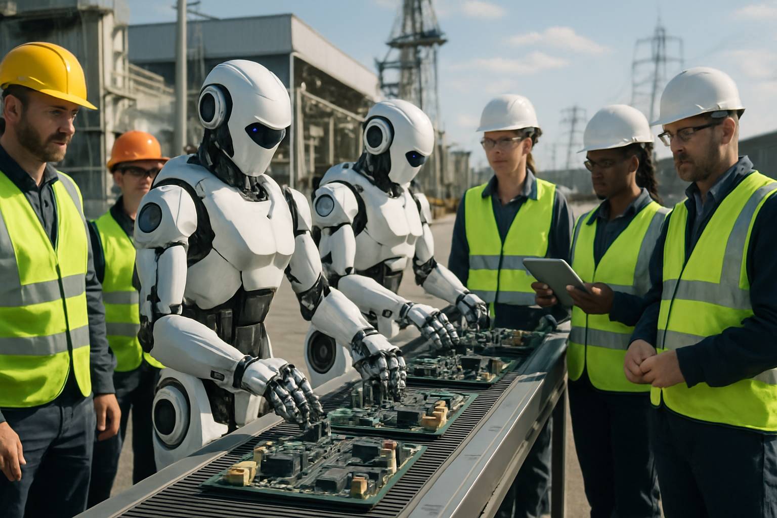
Engineers supervising AI Robotics technology on a modern assembly line.
These declarations excited investors. However, they also triggered skepticism about feasibility. The ambition now anchors discussions for every semiconductor strategist.
Intel Steps Inside Project
On 7 April, Intel posted that it will “help accelerate Terafab’s aim.” Therefore, the company positions its design, fabrication, and packaging strengths as key leverage. Lip-Bu Tan praised the venture as a “step-change” after hosting Musk at Oregon facilities. Furthermore, commentators view the move as validation for Intel Foundry Services.
Yet no binding documents or SEC filings have surfaced. In contrast, Intel’s past partnerships included detailed releases. Consequently, questions persist around equity stakes, capital exposure, and governance. Still, the alliance could funnel leading-edge process knowledge directly into future AI Robotics devices.
Uncertainty clouds the exact manufacturing split. Nevertheless, both firms emphasize speed to volume over traditional incremental ramps.
Capital Scale Meets Reality
Musk cited a US$20–25 billion price tag. However, Morgan Stanley places realistic first-phase costs nearer US$35–45 billion. Bernstein scenarios even project trillions to hit literal terawatt capacity. The gulf illustrates massive capital risk.
Initial Musk estimate: US$25 billion
Analyst base case: US$40 billion
Full terawatt extrapolation: Up to US$5 trillion
Consequently, Tesla’s current 2026 capex excludes Terafab funding. Investors await disclosures on whether SpaceX or external financing will bridge gaps. Moreover, Intel’s balance sheet faces its own fab expansion burdens.
These conflicting numbers underscore financial opacity. Subsequently, stakeholders demand clear milestones before committing additional resources.
Supply Chain Bottleneck Risks
Advanced lithography tools remain scarce. ASML’s EUV systems hold multiyear backlogs. Additionally, skilled fab labor is constrained across the United States. Material suppliers also navigate geopolitical pressures. Therefore, equipment timing may dictate Terafab’s construction pace more than capital.
Terafab must also secure memory processes, high-bandwidth packaging lines, and wafer starts beyond prototype scale. Meanwhile, existing foundries like TSMC and Samsung still dominate 2 nm yields. In contrast, Intel’s internal roadmap aims for 18A nodes by 2027, aligning partially with Musk’s timeline.
These logistical hurdles threaten schedule slippage. Nevertheless, strategic coordination could accelerate domestic AI Robotics supply chains if executed well.
Equipment scarcity highlights execution fragility. However, proactive vendor agreements could mitigate several delays.
Strategic Market Impact Analysis
Should Terafab succeed, strategic ripple effects would follow. Global automakers might reconsider dependence on external chipmakers. Furthermore, U.S. policymakers could view the project as a national security asset supporting sovereign data centers. Consequently, Intel may secure anchor volumes that bolster its foundry push against Asian rivals.
Analysts also note competitive tension with NVIDIA’s GPU dominance. Terafab-built accelerators could shift bargaining power toward Musk-aligned firms in robotics and space computing. Moreover, vertical integration may protect margins for Tesla’s autonomous fleets.
The market stands to gain alternative supply pathways. Subsequently, customers would benefit from diversified AI Robotics silicon ecosystems.
Skills And Certification Paths
A project of this magnitude demands fresh talent pipelines. Semiconductor process engineers, packaging experts, and automation architects will be essential. Additionally, cross-disciplinary teams must understand both factory automation and AI Robotics deployment.
Professionals can enhance their expertise with the AI Robotics™ certification. The program validates competencies in sensor fusion, edge compute, and agile manufacturing. Moreover, credentials help candidates stand out for Terafab hiring waves.
Industry leaders emphasise continuous upskilling. Consequently, structured learning pathways will bridge current talent shortages.
Growing talent will support fab ramp-up. Meanwhile, certified experts will accelerate field adoption.
Outlook And Key Takeaways
Terafab’s vision enthralls technologists, yet many variables remain unresolved. Capital intensity, tool lead times, and governance details require clarification. Nevertheless, the Intel partnership elevates credibility and may hasten practical milestones.
The coming months should reveal financing structures, vendor contracts, and ground-breaking schedules. Furthermore, the outcome will influence broader semiconductor strategy and data centers planning across industries.
These dynamics warrant close monitoring by investors and engineers alike. Consequently, adaptable roadmaps will prove vital.
AI Robotics trends will increasingly intertwine with fabrication strategy. In contrast, firms ignoring supply chain realities risk project stalls.
Proactive engagement, transparent metrics, and skilled personnel remain decisive. Therefore, stakeholders should align now to capture future value.
These insights frame near-term priorities. Meanwhile, Terafab’s evolution will signal the next era for integrated AI Robotics production.
Industry momentum hinges on tangible progress. Nevertheless, informed action today positions enterprises for tomorrow’s intelligent machines.