
AI CERTs
2 months ago
Intel Debuts AI Packaging Test Vehicle for Future Accelerators
Late January 2026 delivered a striking preview of future AI silicon. Moreover, Intel Foundry unveiled an enormous "AI chip test vehicle" to spotlight advanced packaging muscle. The demonstrator spans eight reticle sizes and bundles logic, memory, and power innovation. Consequently, system architects now have a concrete template for multi-chiplet accelerators exceeding current interposer limits. TrendForce analysts say hyperscalers crave alternatives as CoWoS capacity tightens. In contrast, the new platform positions U.S. assembly as a viable path. This article dissects the package, underlying technologies, market context, and production hurdles. Readers focused on Semiconductor Tech strategy will gain actionable detail. Finally, we outline certification resources for navigating legal challenges in AI deployment.
Packaging Demonstrator Explained Clearly
However, Tom’s Hardware stresses the unit is not a shipping accelerator. Instead, the board proves that Intel can assemble four compute tiles beside twelve HBM4 stacks and two I/O dies. Furthermore, EMIB-T bridges interconnect the pieces while UCIe targets 32 GT/s die-to-die links. Therefore, designers can exceed the size limits imposed by a single lithography reticle.
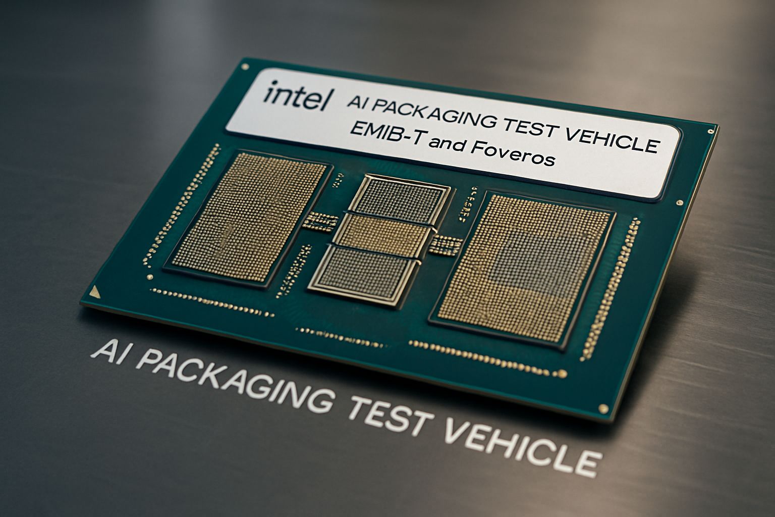
The vehicle validates extreme package scale without monolithic interposers. Subsequently, we examine the silicon building blocks enabling that feat.
Key Silicon Building Blocks
RibbonFET gates on the 18A node drive core logic efficiency. Additionally, PowerVia routes power on the wafer backside to improve current delivery. Foveros stacking options span 2.5D interposers, hybrid bonding, and full 3D die stacking. Meanwhile, Omni MIM capacitors and embedded inductors tame transient loads. Intel pairs these blocks with EMIB-T to balance lateral and vertical density. The combination supports 12 HBM4 towers, each offering multi-terabyte bandwidth. Designers can swap in future HBM4E stacks without altering the bridge pitch. Such flexibility reduces redesign cycles during rapid memory roadmap shifts.
These ingredients form a modular toolkit for heterogeneous accelerators. Nevertheless, market forces will dictate adoption paths. Consequently, we explore those commercial pressures next.
Market Drivers And Impacts
Gartner projects AI semiconductor revenue hitting $397.5 billion by 2029. Furthermore, SEMI expects packaging equipment sales to approach $156 billion by 2027. Hyperscalers seek multi-foundry resilience as demand outpaces TSMC CoWoS capacity. TrendForce notes many teams now evaluate EMIB-T, hoping to avoid interposer area constraints. Importantly, Semiconductor Tech executives value U.S. based assembly for geopolitical risk management. Intel positions its system foundry model as a direct answer to those needs.
- 8× reticle package footprint
- 4 logic tiles on 18A
- 12 HBM4 stacks delivering >4 TB/s bandwidth
- UCIe links at ~32 GT/s
The numbers highlight a strong business case for advanced bridges and backside power. In contrast, technical trade-offs remain significant. Technical comparison with CoWoS reveals those trade-offs.
Technical Contrast With CoWoS
CoWoS relies on a large silicon interposer under every die. Conversely, EMIB-T inserts smaller bridge dies only where needed, improving wafer use. Moreover, package cost scales more gracefully as footprints expand. Thermal paths differ too; EMIB-T leaves substrate areas open for heat spreaders. Semiconductor Tech specialists argue that path length variability complicates signal integrity. Intel counters by highlighting uniform UCIe interfaces and power islands. Signal traces in CoWoS extend across the full interposer, adding capacitance. Bridge based routing shortens critical paths, improving latency for collective operations.
Both paths can reach petabyte memory bandwidth. Nevertheless, bridge approaches promise better scalability. Yet, production brings its own challenges.
Challenges Ahead For Production
Yield remains the largest unknown for eight-reticle assemblies. Additionally, warpage and pump-out risk grow with bigger organic substrates. Cooling 1,000-watt accelerators demands vapor chamber lids and directed flow. Tom’s Hardware warns that thermal margin shrinks when stacked dies share hotspots. Semi-additive build steps also extend cycle time. Intel is building an Arizona advanced-assembly line to tackle throughput and quality. Meanwhile, Semiconductor Tech vendors must update EDA tools for multichip power modeling. Professionals can enhance their expertise with the AI-Legal™ certification to navigate compliance risks in such deployments. Cost models remain uncertain until early yield data reaches public analysts. Nevertheless, equipment suppliers already quote lead times for custom tooling.
Production success hinges on yield, thermals, and supply chain coordination. Subsequently, the broader ecosystem stands to benefit or lose accordingly. Let us examine those ecosystem effects.
Implications For The Ecosystem
Cloud providers gain a potential second source for extreme HBM packages. Furthermore, memory suppliers like SK Hynix secure larger content share per accelerator. OSATs might lose volume if customers move assembly in-house with the new foundry. However, open standards such as UCIe still encourage multi-vendor collaboration. Semiconductor Tech media expect fierce competition to set reference designs before 2027's Jaguar Shores tape-out. Intel aims to prove reliability data within the next year. EDA vendors plan reference flow updates aligned with UCIe 2.0 in 2027. Packaging researchers at ECTC forecast rapid learning curve once early risk builds start.
The ecosystem will watch qualification milestones closely. Therefore, early adopters could lock advantageous supply agreements. We close with final recommendations.
The test vehicle demonstrates practical pathways to enormous, memory-rich accelerators without giant interposers. Moreover, bridge technology, backside power, and smart stacking combine to satisfy emerging AI workload demands. Intel has shown credible manufacturing progress, yet high-yield production still lies ahead. Consequently, engineers and business leaders should monitor qualification updates while strengthening regulatory readiness. Consider pursuing the linked certification to stay ahead of governance hurdles and capture the next wave of Semiconductor Tech growth.


