AI CERTS
3 months ago
UNSW Quantum Scalability Breakthrough Transforms Silicon Qubits
The quantum scalability breakthrough arrives amid fierce competition in silicon-based quantum computing. Earlier attempts linked nuclei only when they shared one electron, limiting expansion. However, UNSW used distinct electrons and tuned their exchange interaction, an approach called electron-mediated entanglement. In contrast, alternative platforms often struggle to combine endurance and integration. Therefore, investors, engineers, and policymakers have begun parsing what this result means for future chip-scale architecture.
Key Experimental Milestone Details
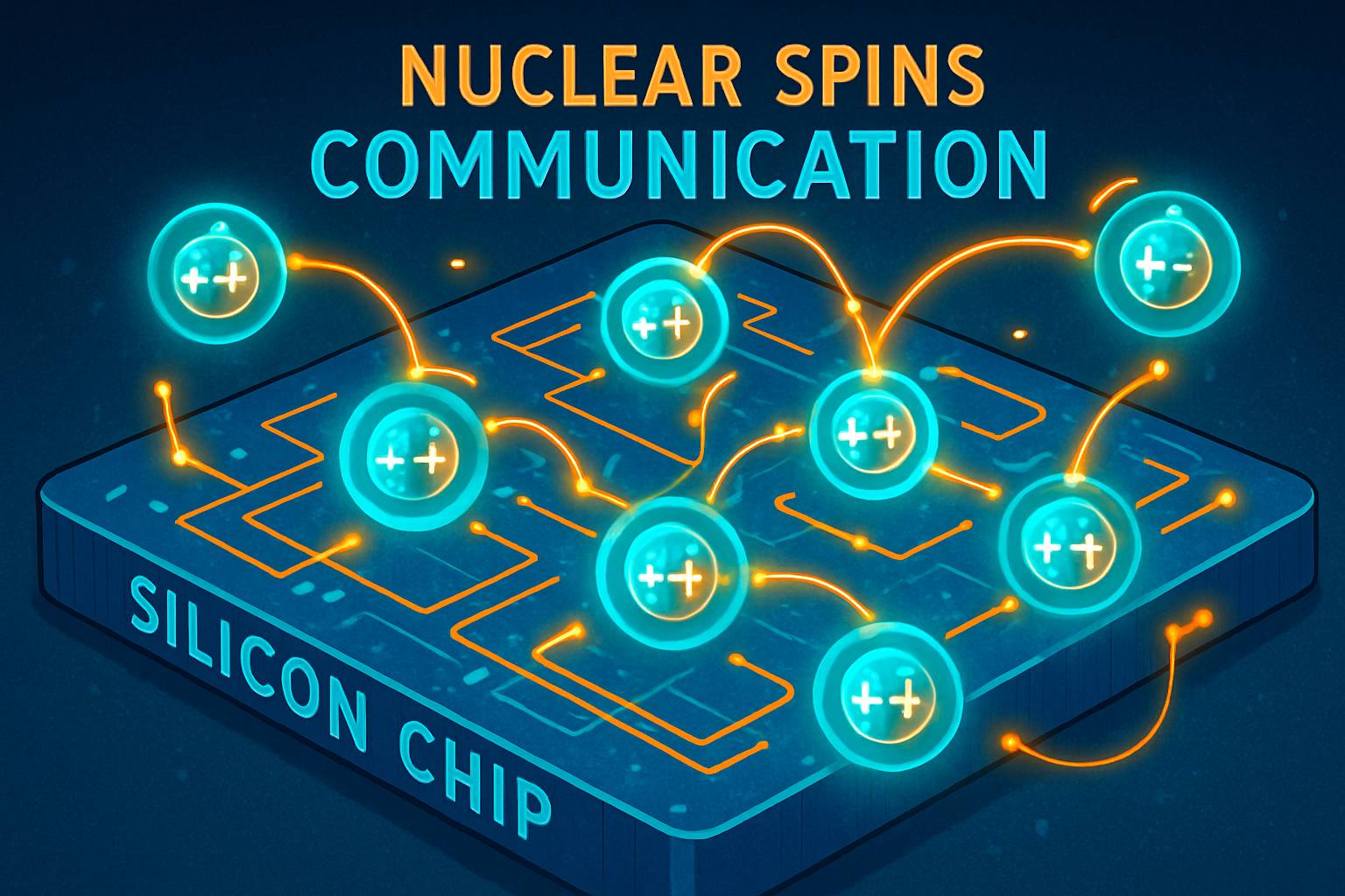
UNSW engineers fabricated an isotopically purified 28Si device that holds two phosphorus donors. Each donor bound its own electron, allowing separate electrical addressability. Furthermore, the electrons could overlap when voltages raised the exchange coupling. That overlap mediated a nuclear-nuclear interaction that delivered the celebrated controlled-Z logic.
During the tests, the team separated donors by about 20 nm, matching modern transistor pitches. Additionally, they achieved single-shot nuclear readout and completed the gate in microseconds. Experts regard this timing as slow compared with superconducting circuits, yet acceptable for nuclear memory roles. Consequently, the demonstrated process underpins the third recorded September 21 discovery in the laboratory’s timeline, reinforcing UNSW dominance.
This section highlights how the gate materialised inside mature silicon tooling. The milestone underscores the third quantum scalability breakthrough pillar: compatibility with existing fabs. These facts set the technical foundation. However, understanding the underlying physics offers deeper insight.
These fabrication facts prove feasibility inside mainstream silicon plants. Nevertheless, explaining the coupling physics clarifies future optimisation.
Physics Behind The Advance
At the heart lies electron-mediated entanglement. Each phosphorus nucleus couples to its resident electron through hyperfine interaction. Moreover, gate voltages expand electron wavefunctions until they overlap, producing an exchange coupling J. Consequently, the electrons briefly form a molecular state that links the otherwise isolated nuclei.
The controlled-Z gate emerges from this interaction. In practice, engineers pulse J for a calibrated duration that rotates the nuclear two-qubit phase by π. Subsequently, the electrons are separated again, preserving nuclear coherence for many seconds.
This physical picture establishes why the device earned another September 21 discovery headline. The mechanism also illuminates why silicon-based quantum computing can combine long memories with CMOS friendliness. Therefore, the quantum scalability breakthrough rests on solid physical ground.
Understanding exchange mediation reveals tunable long-range nuclear logic. Next, we examine the achieved performance numbers.
Performance Metrics And Context
Quantitative evidence matters for any hardware claim. UNSW reported the following core numbers.
- Donor separation: 20 nm, equivalent to 40 silicon atoms.
- Bell-state fidelity: 76% ±5%.
- Concurrence: 0.67 ±0.05.
- Nuclear coherence: previously proven 30 s in similar devices.
- CZ gate time: microseconds, dominated by calibrated exchange pulses.
Furthermore, those figures surpass earlier nuclear entanglement attempts that required shared electrons. However, fault tolerant codes usually demand two-qubit fidelities above 99%. Consequently, further optimisation is mandatory.
The literature provides helpful context. In contrast, superconducting qubits already reach 99.9% two-qubit fidelity but struggle with on-chip density. Meanwhile, silicon-based quantum computing platforms using quantum dots achieve fast gates yet shorter coherence times. Therefore, the UNSW result occupies a unique region of the performance landscape.
Analysts label the experiment a mid-stage quantum scalability breakthrough. Simultaneously, they describe it as a textbook example of electron-mediated entanglement executed inside real chip-scale architecture. Another independent lab even replicated a similar protocol, producing a parallel September 21 discovery press note.
These statistics confirm genuine yet imperfect entanglement. Nevertheless, engineering steps remain before broad scaling.
Scaling Promise And Challenges
Scaling beyond two donors demands precise implantation on dense grids. Moreover, controlling dozens of exchange couplings without cross talk is non-trivial. Cryogenic wiring overhead can also balloon.
Nevertheless, the path leverages existing lithography. CMOS tool sets routinely define 20 nm features, aligning with the donor spacing. Additionally, long nuclear coherence allows relaxed duty cycles, reducing thermal load.
However, fidelity must rise. Error-correcting surface codes expect gate errors below one percent. Engineers therefore plan material purification, pulse shaping, and dynamic decoupling to lift quality. Furthermore, hybrid strategies may integrate faster electron qubits for logic and nuclear qubits for memory.
These realities moderate the excitement around the quantum scalability breakthrough. Yet proponents argue that proven chip-scale architecture compatibility distinguishes this path from others.
Scaling will hinge on implant precision and error improvement. Next, industry voices gauge these challenges realistically.
Industry Reactions And Perspective
Company strategists quickly analysed the result. Quantum-hardware startups highlighted the demonstration as validation of donor-spin roadmaps. Furthermore, investors noted the link to standard fabs lowers capital risk. In contrast, trapped-ion specialists emphasised their superior gate fidelity.
Andrea Morello stated, “The spin of an atomic nucleus is the cleanest quantum object in solid state.” Consequently, his comment resonated across analyst notes. Holly Stemp added that the experiment was like giving nuclei telephones, summarising electron-mediated entanglement in plain language.
Meanwhile, independent academics cautioned that scaling requires thousands of identical donors. Nevertheless, many agreed the quantum scalability breakthrough represents significant momentum within silicon-based quantum computing.
Stakeholders recognise both genuine progress and remaining hurdles. We now distil strategic lessons for decision makers.
Strategic Takeaways For Leaders
Technology executives should monitor donor-based platforms closely. Additionally, procurement teams may begin mapping out dilution refrigerator supply chains. Engineers can prepare by mastering exchange-coupled pulse sequences and low-noise RF design.
Furthermore, professionals can deepen skills through the AI+ Quantum Specialist™ certification. The program covers coherence protection, electron-mediated entanglement, and chip-scale architecture design.
Boardrooms should frame the UNSW work as a mid-term quantum scalability breakthrough. Consequently, budgets can allocate exploratory funding while demanding fidelity milestones. Moreover, partnerships with materials suppliers will be vital.
Leaders gain a roadmap for cautious investment and targeted skill building. Finally, we summarise the entire narrative.
Conclusion And Next Steps
The UNSW experiment marks a decisive quantum scalability breakthrough rooted in proven silicon engineering. Moreover, it links ultra-stable nuclear memories through controllable electron exchange, delivering meaningful fidelity today. Nevertheless, raising gate quality and expanding donor arrays remain essential future tasks. Consequently, engineers must enhance material purity and refine pulse control. Meanwhile, investors should watch for reproducibility metrics and integrated control prototypes. Professionals who pursue advanced credentials will be positioned to guide this evolution. Therefore, explore the linked certification and stay engaged with the fast-moving quantum hardware landscape.


