
AI CERTs
3 hours ago
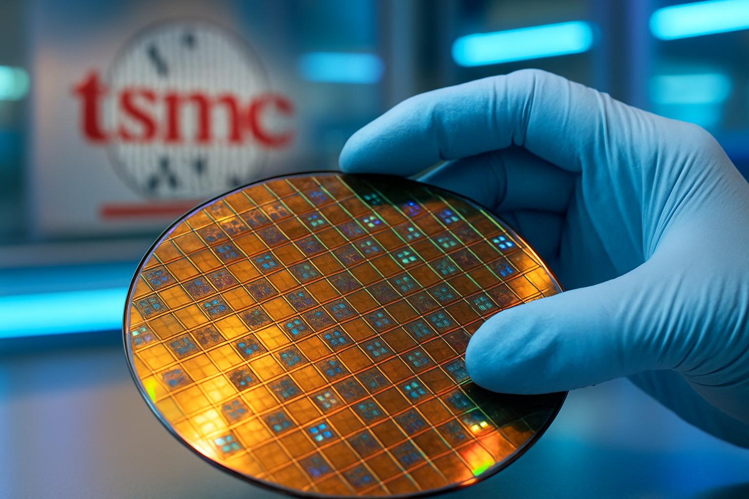
TSMC Starts 2nm Mass Production Amid AI Design Revolution
Chip miniaturization just crossed another threshold. However, industry attention now turns toward the first commercial Gate-All-Around node. TSMC confirmed that its 2nm platform, branded N2, entered volume production during Q4 2025. Consequently, design teams can finally schedule products on a technology once viewed as speculative. Meanwhile, AI design tools have matured enough to keep pace with the aggressive node schedule. Therefore, faster simulations and automated optimizations promise shorter concept-to-tapeout timelines. This article examines the production milestone, supporting ecosystem, and implications for competitive hardware strategies. In contrast, earlier transitions depended on manual tuning that stretched development phases across many quarters. Now, accelerated verification and higher transistor efficiency intersect, potentially reshaping data-center economics and mobile battery life.
GAA Era Finally Arrives
Gate-All-Around nanosheet transistors wrap the channel with gates on all sides for improved electrostatic control. Moreover, this geometry reduces leakage while increasing drive current at minimal voltage. TSMC states that N2 offers 10–15% speed uplift at equal power versus N3E. Additionally, designers can cut power by up to 30% when maintaining former performance levels. The company also claims greater than 15% density gains, enabling smaller die or more on-chip features.
These specifications translate into tangible efficiency increases for both servers and smartphones. Consequently, early adopters gain thermal headroom for aggressive clocks or denser integration. These market incentives fuel a surge in commercial interest, which drives broader demand patterns.
Market Drivers And Demand
AI training clusters crave every joule saved per tera-operation. Furthermore, mobile handset vendors chase longer battery life without sacrificing graphics features. Industry insiders expect 2nm chips to address both priorities by shrinking power budgets.
- Speed gain: up to 15% faster versus N3E
- Power drop: roughly 30% lower at equal performance
- Density boost: over 15% extra logic per square millimeter
- Projected wafer capacity: 50k+ wafers monthly by late 2025, according to TrendForce
- EDA market CAGR: 8–10% through 2028, driven by advanced flows
Moreover, TSMC continues heavy capital expenditure, targeting multiple Taiwanese and overseas fabs for scale. TrendForce projects combined facilities could surpass 130,000 wafers each month by 2026. Nevertheless, equipment lead times and skilled labor availability remain constraining variables.
In short, demand curves appear steep while supply ramps gradually. Therefore, allocation decisions will shape competitive product launch windows. Design efficiency becomes the next differentiator as volume scales.
AI Tools Compress Cycles
AI design tools now permeate every major electronic design automation suite. Synopsys claims up to 30× simulation acceleration when pairing its flows with NVIDIA Blackwell GPUs. Additionally, Cadence reports over 50% of advanced node projects rely on its Cerebrus AI engines. Consequently, optimization loops that once lasted months can conclude within weeks for 2nm chips. TSMC cooperates with these vendors to pre-qualify libraries, ensuring tool output matches fab rules. Many recent case studies presented by TSMC and Synopsys highlight double-digit productivity boosts. Moreover, AI design tools assist in multi-objective trade-offs, balancing power, performance, and area automatically. In contrast, traditional scripting demanded extensive human experience to reach acceptable convergence.
Automated exploration releases scarce engineering capacity for higher-level architectural work. Subsequently, firms can iterate product concepts faster than competitors reliant on legacy flows. However, accelerated timelines amplify risk if manufacturing hurdles emerge.
Capacity Ramp And Risks
Volume production started at Fab 20 in Hsinchu and Fab 22 in Kaohsiung during late 2025. Nevertheless, initial pilot lines shipped only a few thousand wafers each month. TSMC executives forecast continuous output growth through 2027, yet caution that yield learning remains pivotal. Equipment availability also dictates pace. ASML supplies Low-NA EUV scanners today, while High-NA variants arrive steadily but slowly. Therefore, multi-patterning layers add complexity and cost for 2nm chips until High-NA matures. AI design tools mitigate some complexity by detecting pattern hot-spots before masks reach the fab. TSMC also invests in advanced packaging to complement node scaling. Geopolitical licensing uncertainties add further planning challenges for cross-border fabs.
Collectively, these factors could delay full utilization if not managed carefully. Yet, proactive collaboration across suppliers keeps contingency options open. Competitive dynamics further intensify the pressure to resolve such bottlenecks quickly.
Competitive Landscape Shifts
Samsung Foundry and Intel Foundry Services both chase similar nanosheet timelines. In contrast, their risk production windows trail TSMC by several quarters according to press estimates. Moreover, customer loyalty remains fluid because allocation priorities depend on yield, price, and schedule. Big buyers of 2nm chips, including Apple and NVIDIA, reportedly negotiate multi-year wafer commitments. Consequently, whichever supplier scales fastest gains lucrative AI accelerator volume. Furthermore, differentiated AI design tools bundled with foundry reference flows deepen customer lock-in. Meanwhile, equipment shortages could allow early leaders to raise prices without immediate customer flight.
Competitors must therefore innovate across process, packaging, and software simultaneously. Subsequently, partnerships spanning EDA, compute, and equipment become strategic necessities. Executives now seek actionable guidance for navigating this multifaceted shift.
Strategic Takeaways For Leaders
TSMC production progress signals that advanced capacity will soon influence data-center energy budgets materially. Consequently, system architects should model power reductions and adjust cooling infrastructure budgets early. Integrating AI design tools from project inception can shave months off launch schedules and minimize re-spins. Additionally, procurement officers should monitor wafer allocation negotiations at least two quarters ahead. Early price signals for 2nm chips often crystallize once high-volume customers lock agreements. Professionals can enhance strategic foresight with the AI Executive™ certification. Moreover, such credentials formalize knowledge of AI hardware roadmaps and cross-industry collaboration patterns.
Leaders who align technical, financial, and talent strategies will capitalize on this node transition. Therefore, deliberate preparation converts uncertainty into competitive advantage. The concluding section distills the article’s principal insights.
Conclusion And Future Outlook
TSMC has moved 2nm technology from laboratory to production scale. Meanwhile, AI design tools shrink design timelines and ease complexity burdens. Consequently, power efficiency and time-to-market improve together, not in isolation. Nevertheless, equipment scarcity, yield uncertainty, and geopolitical friction remain material risks. Therefore, continuous monitoring of capacity announcements and tool benchmarks is essential. Act now by exploring the linked certification and stay prepared for the accelerating semiconductor race.


