
AI CERTs
2 hours ago
TSMC Japan Expansion Targets 3nm Manufacturing in Kumamoto
Japan is poised for another manufacturing leap. TSMC Japan Expansion dominated headlines after reports of a US$17 billion upgrade for the second Kumamoto fab. Furthermore, journalists say the node target shifted from 6 nm to 3nm logic. Consequently, policymakers view the move as vital for economic security and AI leadership. C. C. Wei briefed Prime Minister Sanae Takaichi on 5 February, underscoring shared goals. However, TSMC has not issued a formal statement confirming the figure. Meanwhile, Reuters and Yomiuri cite executives for verification. Additionally, investors track how the larger commitment fits a 2026 capex plan possibly reaching US$60 billion. Together, these factors frame a pivotal moment for global chips markets.
TSMC Japan Expansion Overview
The reported upgrade marks the second major shift for the Kumamoto program since 2024. Initially, the plan focused on 12-28 nm automotive chips for Sony and Denso partners. Subsequently, management proposed 6 nm capacity with capex near US$12.2 billion. Now, local outlets describe 3nm lines needing about US$17 billion. Moreover, the factory remains under JASM, a TSMC-majority venture with Sony, Toyota and Denso. Industry observers note that the TSMC Japan Expansion also hedges geopolitical risk by dispersing capacity. These revisions illustrate rapid roadmap evolution. Consequently, deeper financial analysis becomes essential for upcoming negotiations.
Understanding Advanced 3nm Technology
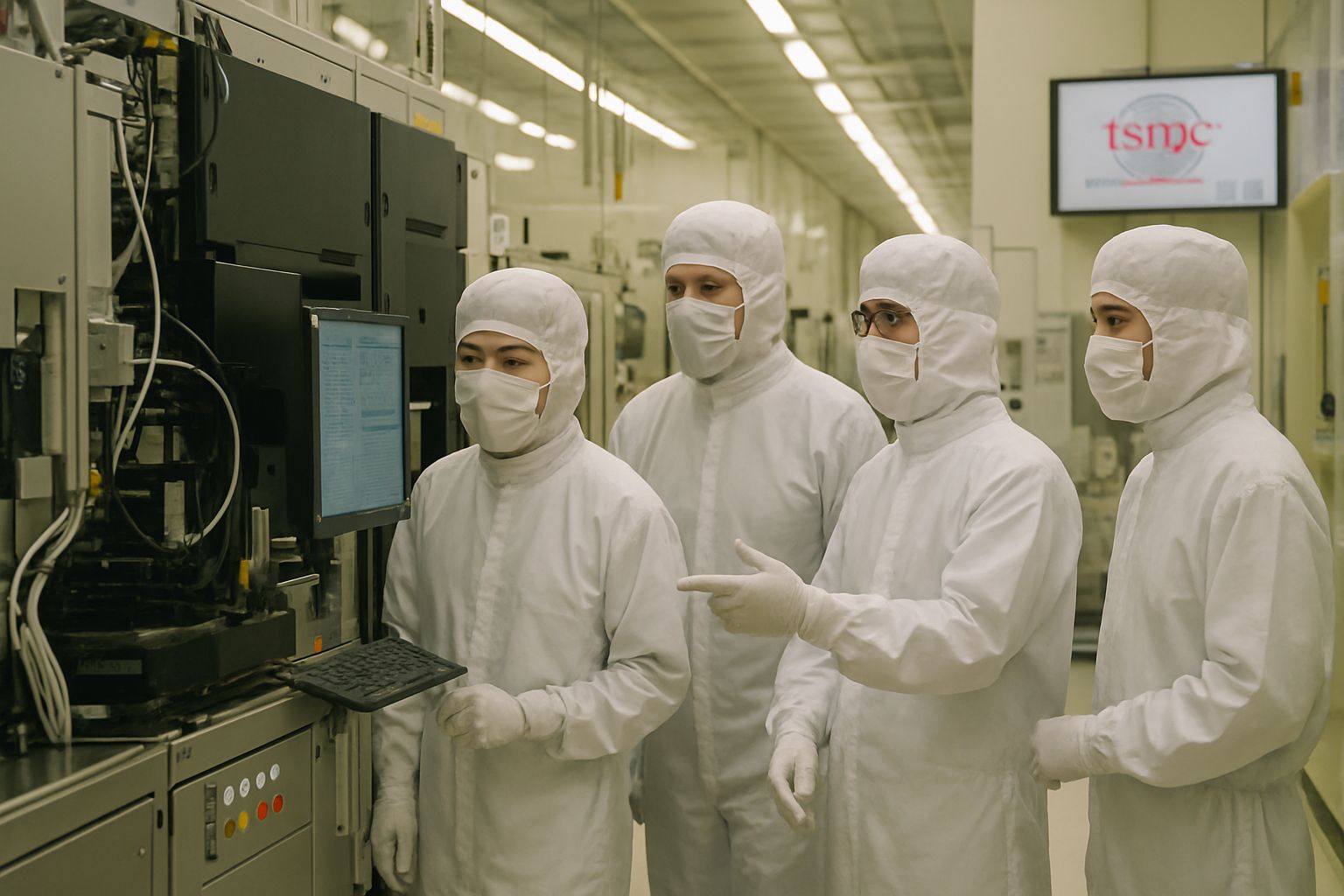
3nm denotes a process node delivering higher transistor density and lower power than 5 nm predecessors. Therefore, the node suits AI inference, elite mobile and autonomous driving workloads. In contrast, older 12 nm lines serve less demanding control chips. Producing at 3nm requires extreme ultraviolet lithography, specialized materials and precise contamination control. Experts argue the TSMC Japan Expansion will make Japan only the second nation hosting commercial 3nm capacity outside Taiwan. Additionally, regional universities expect fresh research partnerships. Such technical complexity creates both opportunity and risk. Nevertheless, early mastery could position Japan as an indispensable advanced-node supplier.
Investment Figures And Context
Financial details remain fluid. Reuters cites a provisional US$17 billion allocation, eclipsing the US$13.9 billion noted during October 2025 construction updates. Meanwhile, the February 2024 release placed combined JASM funding above US$20 billion. Financial analysts believe the TSMC Japan Expansion will test investor appetite for escalating capital intensity.
- Initial second-fab estimate: US$12.2 billion for 6 nm capacity
- Revised 2025 estimate: US$13.9 billion as construction began
- Current reported figure: US$17 billion targeting 3nm
- Japan fiscal subsidy pool: ¥1.23 trillion for semiconductors and AI
Moreover, market watchers forecast total 2026 spending of US$50-60 billion across all TSMC sites. Therefore, the TSMC Japan Expansion represents roughly one-third of the yearly outlay. These numbers underline breathtaking capital demands. Consequently, subsidy negotiations will likely intensify during coming months.
Policy And Subsidy Landscape
Japanese lawmakers regard advanced semiconductors as critical to national resilience. Consequently, the government allocated record budgets to attract frontier fabs. METI officials are reportedly evaluating fresh incentives tied to the new 3nm objective. Simultaneously, Tokyo backs Rapidus, a domestic foundry targeting 2 nm technology in Hokkaido. Nevertheless, officials insist the initiatives complement rather than compete. The TSMC Japan Expansion gains momentum because it delivers immediate scale and proven engineering. Policy alignment can accelerate site readiness. However, overlapping subsidies may spark debate over taxpayer returns.
Operational Timeline And Risks
Construction began in late 2025 after local permitting hurdles. Yet July 2025 reports suggested a possible delay to 2029. Subsequently, company teams revised schedules, aiming for initial 2027 output if upgrades proceed. Logistics, training and housing shortages in rural Kumamoto remain pressing. Furthermore, advanced 3nm production lines need technicians experienced with EUV tools. Any talent gap could slow the TSMC Japan Expansion. Such risks demand vigilant project management. Consequently, contingency planning has become central to the Kumamoto build.
Implications For Global Supply Chains
Locating 3nm production in Japan diversifies global chip supply away from Taiwanese earthquake and geopolitical exposure. Moreover, automotive clients gain proximity, shortening logistics cycles. In contrast, U.S. fabs in Arizona target different customer mixes and timelines. Therefore, the TSMC Japan Expansion strengthens redundancy while avoiding over-concentration. Distributed capacity supports resilience during demand spikes. Consequently, customers benefit from multi-region sourcing.
Talent Development And Certifications
A skilled workforce underpins every modern fab. Kumamoto universities are launching curricula covering EUV maintenance and AI-driven yield control. Additionally, professionals nationwide can enhance expertise with the AI Engineer™ certification. Such programs align with leadership goals to embed advanced manufacturing know-how domestically. The TSMC Japan Expansion will employ thousands across engineering, logistics and quality roles. Human capital shapes competitive advantage. Therefore, continuous training remains paramount for sustained 3nm success.
The reported upgrade signals a strategic inflection for Japan’s technology landscape. Moreover, it elevates national ambitions from legacy chips to frontier semiconductors. Financial, policy and talent factors still require confirmation, yet momentum appears strong. Consequently, the TSMC Japan Expansion could redefine regional supply networks and accelerate AI innovation. Nevertheless, schedule risk and subsidy scrutiny persist. Stakeholders should monitor official disclosures and pursue skills development to seize emerging roles. Explore our certification resources to stay ahead in the evolving semiconductor arena.


