AI CERTS
2 months ago
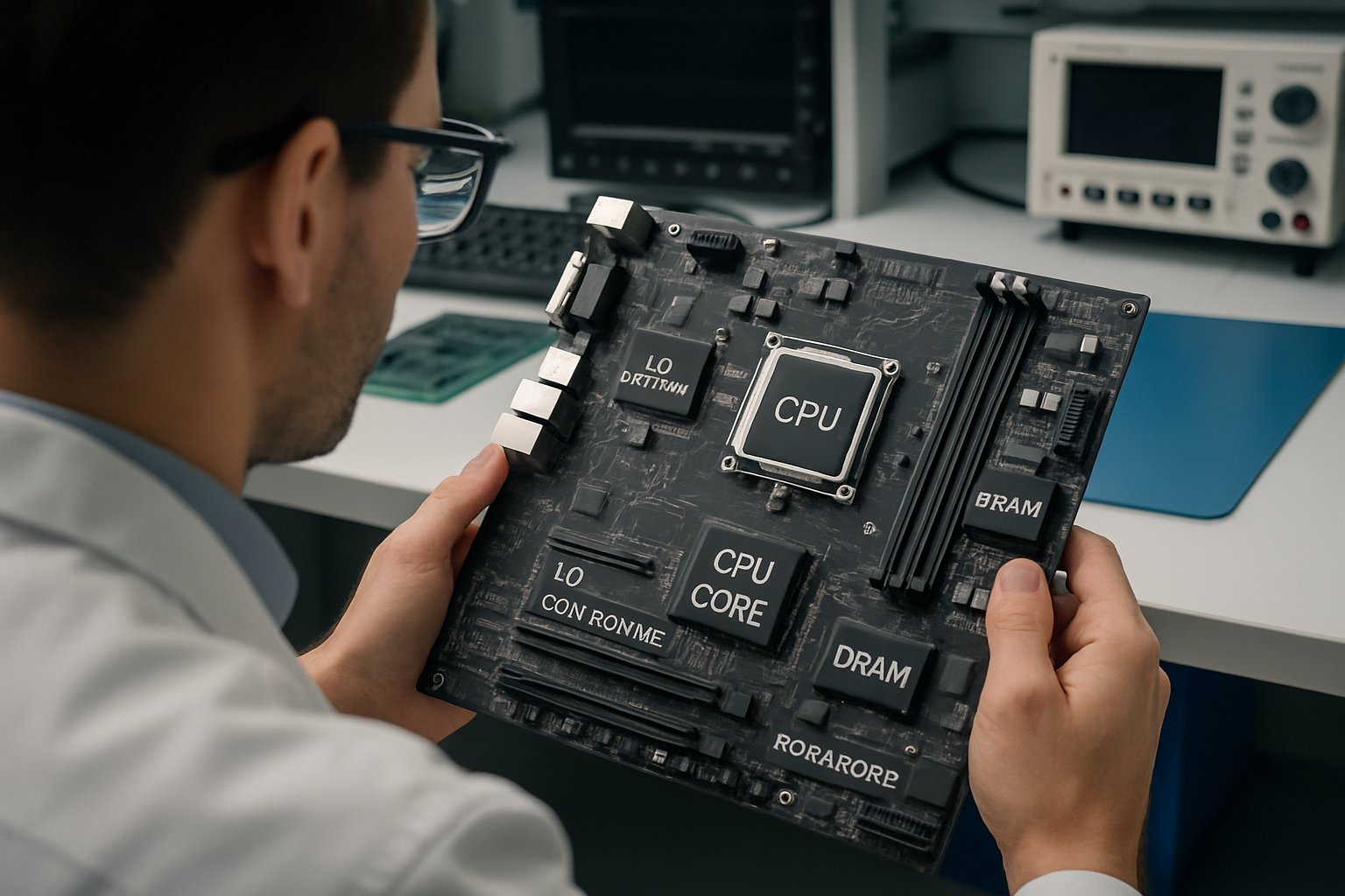
Positron Atlas Rivals H100 via Efficient Chip Architecture Design
Moreover, investors have poured more than $300 million into the company since 2023. Industry veterans therefore wonder whether a fresh Chip Architecture Design can finally dent NVIDIA’s dominance. This article dissects the announcement, evaluates the engineering claims, and frames what must still be verified.
Data Center Energy Stakes
Training models remains costly, yet inference runs continuously in production workloads. However, inference electricity often exceeds 70% of total operational spend for generative AI services. Utility upgrades and higher PUE rates force operators to seek efficient hardware. In contrast, lowering power draw frees up rack capacity without facility expansion.
The economic stakes therefore incentivize alternatives promising superior perf-per-watt. These realities set the stage for Positron’s bold marketing push toward efficiency. Let us examine the specific claims surrounding Atlas.
Positron Atlas Bold Claims
Positron states that one Atlas node delivers 280 tokens each second for every user. Meanwhile, an eight-GPU DGX H200 reportedly reaches only 180 tokens per user. Consequently, Positron cites a threefold performance-per-watt advantage at 2,000 watts versus 5,900 watts. The company also touts greater than 93% memory bandwidth utilization, far above typical GPU figures.
Reuters, TechCrunch, and Tom’s Hardware have repeated these numbers while stressing they remain vendor supplied. Nevertheless, major enterprises, including Cloudflare, are piloting the platform in production-like settings. Additionally, CEO Mitesh Agrawal argues that domestic manufacturing adds geopolitical value.
Atlas therefore appears attractive on paper. However, numbers require context and independent replication before conclusions. Understanding the underlying Chip Architecture Design will clarify potential advantages.
Modern Chip Architecture Design
Positron claims its architecture reallocates die area from compute cores to high-bandwidth memory controllers. Consequently, transformer inference, usually memory bound, benefits from the shift. The company suggests that conventional GPUs waste energy fetching weights rather than executing operations. In contrast, Atlas places SDRAM physically closer to the compute fabric, reducing latency.
Furthermore, the design unifies scheduling and networking, enabling deterministic token throughput. Such decisions mirror trends in other inference ASICs, yet Positron emphasizes flexibility similar to FPGAs. Nevertheless, confusion persists over whether shipping silicon is fully custom or relies on FPGA overlays.
The Chip Architecture Design therefore prioritizes memory efficiency over sheer FLOPS. That focus explains many of the published perf-per-watt numbers. Still, memory specialization introduces its own trade-offs, discussed next.
Memory Bandwidth Focus Area
Tom’s Hardware notes Atlas reports 93% sustained bandwidth utilization. Moreover, early customer logs corroborate minimal stalls during autoregressive decoding. By contrast, GPUs typically operate between 10% and 30% utilization in similar tests. Therefore, Positron’s controller design could translate directly into lower idle power.
- 280 tokens per second at 2 kW envelope
- 93% memory bandwidth utilization in transformer inference
- 3.5× performance per dollar versus H100
- Domestic fabrication planned at TSMC Arizona
These figures highlight advantages tied to data movement efficiency. However, raw numbers still lack peer-reviewed validation. Independent benchmarking becomes critical for enterprise adoption.
Verification And Key Caveats
Independent journalists consistently caution readers about vendor trials. Interestingly, Tom’s Hardware flagged possible FPGA use that skews power comparisons. Furthermore, measurement points vary; some firms meter at wall, others inside chassis. Therefore, identical workloads and standardized setups are essential. A rigorous Chip Architecture Design audit must precede large enterprise rollouts.
SemiAnalysis analysts propose third-party labs replicate Llama-3.1 tests with transparent logs. Meanwhile, Positron has promised to release methodology details shortly. NVIDIA representatives declined comment when asked about the comparison.
Verification uncertainty tempers enthusiasm. Nevertheless, clarity could arrive before large procurement cycles. Roadmaps matter alongside validation.
Roadmap And Future Outlook
Positron plans a second-generation ASIC called Asimov for 2026. Additionally, the firm targets doubled memory capacity and bandwidth. If successful, Asimov could widen the efficiency gap further. Asimov will refine the Chip Architecture Design for even denser memory fabrics.
Funding appears sufficient; a $230 million Series B closed in 2026. Consequently, manufacturing partners and supply chain scaling look feasible.
The roadmap aligns with rising inference demands. However, competitive responses from NVIDIA and hyperscalers remain inevitable. Economic forces will shape final market impact.
Economic And Ecosystem Impact
Switching away from NVIDIA involves more than silicon. CUDA libraries, vendor support, and existing workflows create inertia. In contrast, Positron promises PyTorch compatibility and drop-in APIs. Moreover, domestic supply resonates with public sector buyers. Teams trained in Chip Architecture Design can optimize kernels for the new fabric.
Lower power use also reduces heat, enabling higher rack density. Consequently, operators may defer costly substation upgrades. Enterprises can further validate skills through the AI Architect certification, ensuring teams exploit new hardware efficiently.
Ecosystem readiness will influence adoption pace. Nevertheless, efficiency economics cannot be ignored. A balanced view now emerges.
Conclusion And Next Steps
Positron delivers an intriguing efficiency narrative backed by sizable funding and early customer trials. Moreover, claimed threefold perf-per-watt gains tempt operators facing soaring energy bills. Nevertheless, only transparent benchmarking will confirm whether the Chip Architecture Design truly eclipses H100 systems. Consequently, technology leaders should monitor forthcoming lab reports while preparing migration plans. For deeper readiness, pursue the linked AI Architect credential and stay ahead of evolving inference hardware.


