AI CERTS
4 weeks ago
Optical Computing AI Achieves Single-Shot Light Tensor Processing
Consequently, engineers and investors need a clear roadmap. This article unpacks the Light-based method, highlights numbers, and assesses readiness for large-scale applications. Furthermore, it situates the advance within broader photonic initiatives from Aalto and industrial players. Expect practical guidance, balanced caveats, and strategic actions for teams exploring Optical Computing AI solutions.
Photonics Shift Accelerating Rapidly
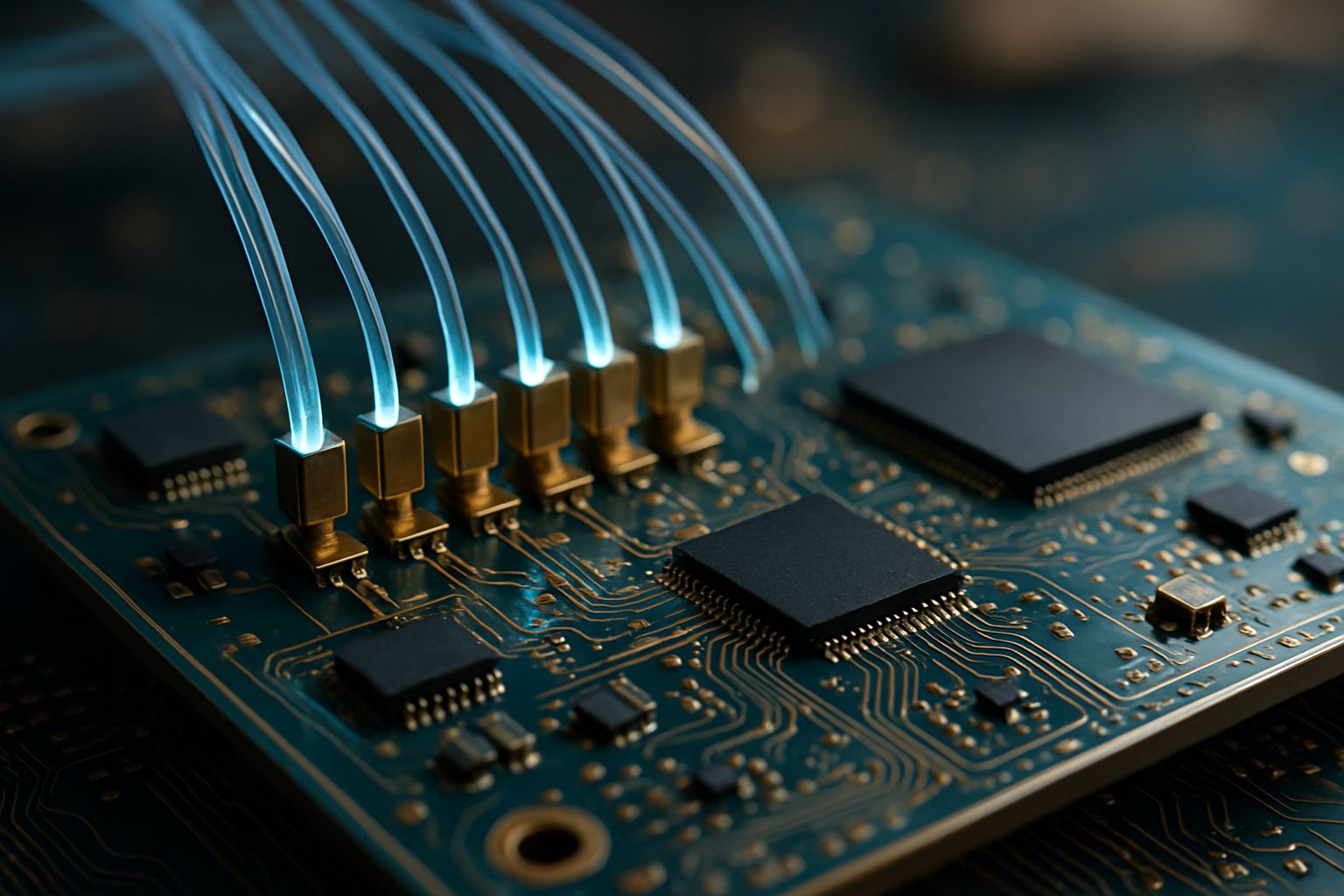
Photonic computing has simmered for decades. However, past designs demanded multiple optical passes, erasing latency advantages. Parallel Optical Matrix–Matrix Multiplication, or POMMM, removes that bottleneck with one light propagation. Moreover, the device releases results simultaneously, creating true wavefront-level parallelism.
Lead authors from Shanghai Jiao Tong University teamed with Aalto University to fabricate a tabletop prototype. Coherent light beams encoded both amplitude and phase, representing full matrices in spatial patterns. Consequently, downstream lenses executed Fourier transforms while a camera captured the finished product instantly. Observers liken the approach to analog Waves weaving mathematics into photons.
The single-shot design revives Optical Computing AI ambitions with tangible laboratory evidence. Therefore, understanding its internal mechanics becomes essential.
Inside Single Shot Process
Key Statistics Snapshot Now
Inside the setup, two spatial light modulators imprinted matrices A and B onto orthogonal beam regions. Meanwhile, a cylindrical lens pair produced necessary Fourier optics, enabling convolution in momentum space. Subsequently, another lens re-imaged the interference pattern onto a CMOS sensor, effectively reading the tensor product. The entire optical path measured under 30 centimeters, yet it executed 256-square multiplications in microseconds.
- Prototype energy efficiency: approximately 2.62 GOP per joule using off-the-shelf parts.
- Largest demonstrated multiplication: 9,216 x 9,216 elements processed in one shot.
- Projected on-chip efficiency: orders of magnitude higher after photonic integration, authors claim.
Therefore, the demonstration offers a concrete building block for Optical Computing AI pipelines. These metrics showcase promising throughput despite improvised laboratory hardware. Consequently, stakeholders now examine practical performance against electronic benchmarks.
Performance Numbers And Caveats
Performance headlines excite, yet context matters. For comparison, modern GPUs reach tens of tera operations per joule under ideal loads. Nevertheless, POMMM numbers exclude electrical I/O and analog-to-digital conversion overheads. Moreover, the camera readout limited frame rates, capping measured throughput. Such gaps must close before Optical Computing AI outperforms GPUs in production.
Noise, thermal drift, and discretization further constrain precision. In contrast, electronic accelerators support high bit depths with mature error correction. Authors propose calibration routines and wavelength multiplexing to mitigate such issues. Furthermore, nonlinear activations still require hybrid electronic loops, adding complexity.
Overall, excitement persists yet realism tempers expectations. Therefore, industry observers track commercial roadmaps closely.
Industry Context And Timelines
Major photonic startups already court hyperscale buyers. Lightmatter, Ayar Labs, and others ship optical interconnect prototypes compatible with advanced packaging. Global vendors already prepare Optical Computing AI roadmaps to court cloud providers. Consequently, the authors estimate three to five years for integrated POMMM chips. Meanwhile, TSMC's COUPE interface demonstrates co-packaged lasers linking silicon and Waves of data.
Aalto researchers emphasise platform agnosticism, arguing any waveguide material could host the design. Moreover, GPU-trained weights port directly, lowering software friction. Investors therefore weigh the chance of leapfrogging incremental GPU gains. In contrast, skeptics recall earlier optical ventures that stalled at packaging hurdles.
Timelines hinge on integration successes and supply-chain maturity. Consequently, Optical Computing AI commercialization now hinges on photonic packaging maturity.
Challenges Facing Photonic Integration
Building dense amplitude-phase modulators remains priority one. However, low-loss materials and CMOS compatibility rarely coexist. High-speed photodetector arrays must also shrink dark currents while preserving bandwidth. Additionally, optical I/O consumes board space and alignment budgets. Waves of crosstalk also threaten precision during high-density interference.
Consequently, co-packaged lasers and optical sockets attract intense development funding. In contrast, mature electronic sockets enjoy decades of cost optimization. Moreover, reliability testing must address vibration, temperature cycles, and moisture. Nevertheless, recent progress in silicon photonics suggests feasible paths forward.
These hurdles could delay deployments if left unresolved. Therefore, practitioners need actionable guidance.
Roadmap For Tech Practitioners
Teams exploring Optical Computing AI should begin with workload profiling. Identify linear layers dominating latency and power. Subsequently, evaluate tolerance for analog noise and reduced precision. Moreover, track photonic vendor roadmaps and public prototypes.
Professionals can enhance their expertise with the AI+ Quantum Robotics™ certification. Consequently, certified engineers will understand optical stack dependencies and integration workflows. Additionally, maintain relationships with Aalto groups and Lightmatter engineers for early test access. Finally, allocate small budgets for benchmarking optical evaluation kits when released.
- Map tensor-heavy layers to candidate photonic cores.
- Plan hybrid activation strategy between optics and electronics.
- Prepare data pipelines matching sensor frame formats.
These steps position teams for rapid adoption once hardware matures. Meanwhile, ongoing research deserves continued attention.
Conclusion
The POMMM demonstration signals a pivotal moment for photonic hardware. Moreover, measured throughput, even with improvised parts, validates core physics. Industry traction from Ayar Labs and Lightmatter indicates growing supply-chain confidence. Nevertheless, packaging, detectors, and nonlinearities remain gating factors. Consequently, sustained investment will decide whether Optical Computing AI escapes prototypes. Practitioners should profile tensor workloads, follow Aalto updates, and engage emerging standards. Finally, begin certification journeys to stay competitive in a rapidly evolving photonic era. Visit the certification portal today and position your team for light-speed innovation.


